Center for VLSI and Embedded System Technologies

Low Power Analog and Digital Circuit Design :
Consumers have discovered that they couldn't live without battery-powered handheld devices (cell phones,
tablets), therefore low-power design became the top priority that it remains today. The driving forces
behind the developments in low power CMOS circuit designs are portable applications requiring low power
dissipation and high throughput, such as notebook computers, portable communication devices and personal
digital assistants (PDAs).
In Digital, Moore's Law helped a great deal, but so did a host of other clever innovations including multiple clock and power domains, dynamic voltage and frequency scaling, optimizing algorithm for adjusting W/L ratio, power gating, and multiple sleep states. All of these techniques are highly effective for digital designs but won’t work in the analog domain.
In CVEST, low power analog and digital circuit design is an active and growing research area which includes the innovations and different approach to design analog and digital circuits in low power while maintaining the required specification and optimizing digital circuits with different techniques to work under minimum power.
Analog and Mixed Signal Design:
The world remains stubbornly analog, as do humans. Devices such as cell phones, laptops works on
battery— which contain a multitude of sensors as well as analog outputs— are challenged to process
analog data while retaining signal integrity and low power consumption. Power is always traded off for
speed (bandwidth), resolution (linearity), and low noise (SNR) therefore designing the analog circuits
under low power and achieving all the constraints is a great challenge but also a great learning and
understanding of circuits.
Analog-Mixed Signal Circuit Design research at CVEST focuses on the modeling, designing, fabrication and testing of chip. Analog circuit design research in CVEST targets the low power circuit designing and layout designing following with the fabrication and testing of the respective IC. The aim is to provide low-cost, low-power and high yield designs used in automobile, implantable bio medical system, energy harvester, wireless sensor nodes and IoT based applications etc. The research also comprise the mathematical modeling of MEMS and CMOS circuitry (ex. linear resistance, composite pair using CMOS etc).
A reference in analog is that outputs a constant voltage or current w.r.t. to temperature and supply change hence used as reference in different systems. Many voltage and current references had been designed for their respective system having specification from 400mV to 1.2V and 10nA to 10uA for temperature range of -55oC to 125oC under power of few nW to tens of uwatt with high supply rejection and process insensitivity.
A voltage having PTAT/CTAT characteristic can be used for sensing temperature following the linearity between temperature and voltage. CMOS based temperature sensing is most efficient in terms of cost and area therefore are designed using CMOS technology having good supply rejection and process insensitivity (otherwise requires trimming). Different low power temperature sensor architecture had been developed in CVEST lab, a) Composite pair based Temperature sensor (consume power in nW), b) BJT based sensor (for high linearity and speed), c) Resistance based temp sensor (uses linear characteristic of resistance w.r.t. temperature). Temperature sensors designed in lab achieve the temperature coefficient of 10ppm ± 5ppm, with modified slope for military temperature range of -55oC to 125oC under 100nW of power (compatible for IoT sensors, energy harvester system).
Op amp’s being the most integral building block of analog are designed to satisfy
various design constraints. These include conventional single stage and miller
compensated two stage op amp for applications requiring moderate gain, Folded cascode op
amp with gain enhanced boosting for applications requiring high gain, rail to rail op
amps for high swing, Conventional high speed op amps consuming higher power consumption,
Dynamic op amps that consume lower current in off state and higher current under
requirement.
Comparators being the most essential building block that converts analog signals to
digital domain are designed to meet the various design constraints. Some of these
include always on comparators with supply and temperature insensitive delays for
comparator based voltage to time converters, Always on comparator with hysteresis,
Conventional Latched comparators for SAR ADC, Low kickback noise latched comparator for
low power applications.
Designed a fully integrated 128Hz RC time constant based oscillator in tsmc_180nm for slave nodes in connected modes of Bluetooth Low Energy (BLE) or 802.15.4 networks, especially at low duty cycles. A comparator offset cancellation scheme is used to achieve temperature stability improvement leading to an accuracy of +/- 0.2% to +/- 0.5 % over -55 to 125 C. Subthreshold operation and low swing oscillations resulted in ultra low power consumption of ~10nW. The architecture also provides timing noise suppression, leading to remarkable reduction in long-term Allan deviation.
Process sensing includes sensing the various process corners so that they can be given as inputs to the Auto calibration system. Efficient process sensing translates to efficient auto calibration systems. A process sensing system is developed that could sense ss, tt, ff, sf, and fs corners.
Trimming and calibration is usually required in analog circuits because of change in functionality due to process variation. Trimming helps to make the circuit come back to its original value by cancelling the effect of process. Voltage reference, Current reference, temperature sensor etc are sensitive to process variation i.e. their respective value changes with process (ss, ff, tt, sf, fs). Therefore a manual trimming or self/auto trimming is required to make the designed circuit come back to its original value. Manual trimming is calibrating IC from outside and most preferably done as it is most accurate but cost hungry. While auto trimming is done by designing trimming circuit such that it automatically sense process using process sensor or some feedback which trim the circuit to original value. It is cost effective but require complex designing and not as efficient as manual trimming.
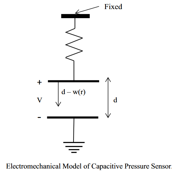
TThe research work is based on Micro-electro-mechanical system (MEMS) based clamped circular capacitive pressure sensor with pre-stressed diaphragm made of polysilicon material with compressive residual stress. The small deflection theory of plates is utilized for designing the capacitive pressure sensor for blood-pressure measurement of the range 1.0 bar to 1.4 bar. The work includes the mathematical modeling of capacitive pressure sensor devices.
Power management IC is the integral part of any chip.Which takes care of power conversions,protection from sudden supply changes etc.LDO is the integral part of PMIC which takes care of providing ripple free, highly stable output voltage. Here in CVEST we aim at designing LDO for various specifications like:-
Targeted Applications: Energy Harvester, wide angle cameras,PMIC for mobiles etc.
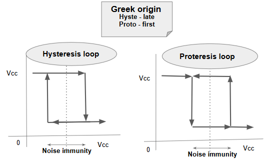
Bistability is a well-known phenomenon and is a widely applied concept while implementing electronic Switches. This is due to the fact that it has exactly two stable outputs irrespective of the range of input given. Bistability along with hysteresis is proven to be very useful concepts in building a noise immune stable circuits.
But hysteresis is defined as a phenomenon where effect lags behind the applied force, hence it adds delay to the system. Our work explores the possibility of building a system, followed by a circuit which can possess both bistability and noise immunity without any delay or if possible an advancement in transition time compared to a hysteretic circuit or a basic inverter. This newly mentioned phenomenon is also seen in a good number of natural process, and it is called as Proteresis. Both proteresis and hysteresis are greek origin words where Proto means ahead and Hyste means late. The main motivation for this work is that in nature we observe that most of the things exist in pairs like high, low; Negative logic, positive logic; cause, effect; clockwise spin, anti-clockwise spin; etc. And this work explores the possibility of the opposite pair of hysteresis and it's possible contribution in electronics.
Mixed Signal Circuit Design:This area focuses on designing data converters including voltage to digital converter, voltage to time & frequency converter, digital to analog converter, nyquist converters and system level designs such as temperature, humidity and pressure to digital converter using CMOS and MEMS circuit etc.
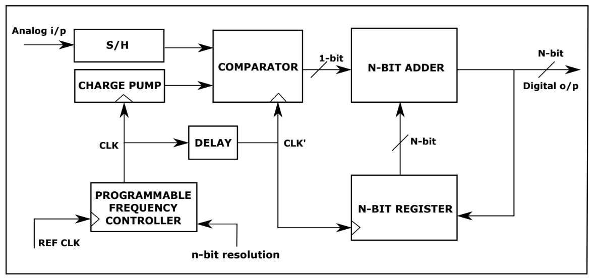
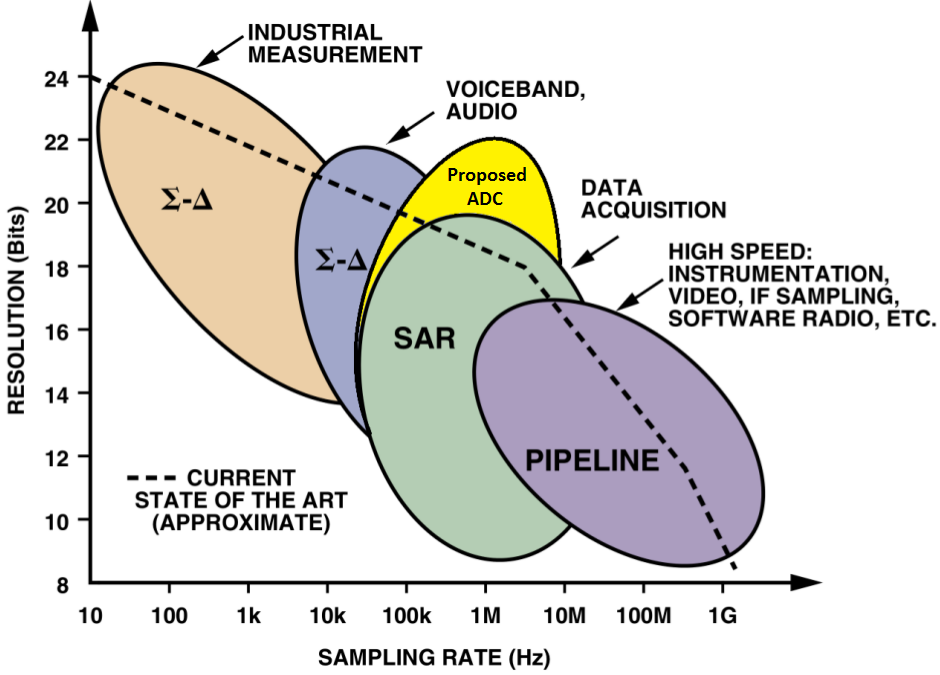
Analog-to-Digital Converter (ADC) is considered one of the most essential blocks in Software Defined Radio (SDR), Ultra-Wide Band (UWB) receivers, biomedical applications,and embedded system. Decreasing the percentage of the analog part and increasing the percentage of the digital part in integrated circuits is the current trend and is highly recommended to maximize the benefit of the unceasing CMOS technology scali The time based analog to digital converters being digitally oriented gets benefited with scaling as opposed to conventional ADC’s. The Time based ADC converts the analog signal to a time delay representation through a Voltage-to-Time Converter (VTC). Then, the time-represented signal is converted to digital code through a Time-to-Digital Converter (TDC). Another type of time based ADC involves converting voltage to frequency followed by frequency to digital conversion.
These type of ADC’s find use in multiple channel applications. However the fact that these can be designed for low power is exploited in many recent ultra low power architectures. A 8 bit wilkinson Analog to digital converter is implemented for ultra low power temperature sensing applications. This consumes a power of less than 40nW with very less fluctuation in performance for military temperature range.
This ADC architecture’s idea come from Flash ADC and developed further from SAR and Counter type ADC.
Temperature sensors find plethora of applications like environment monitoring, biomedical, heat monitory in processors, etc. However recent advancement in technology demands sensors that could work with very low power so that they could be powered by energy harvesters. A sub 100nW temperature sensor is implemented for military temperature range. A very high PSR and wide supply range is an added advantage to the design. Moreover process spread is decreased by adopting a process sensor circuit which could automatically sense the process data and calibrate the sensor.
Digital and Mixed Signal Design: Very-large-scale integration (VLSI) is the process of creating an integrated circuit (IC) by combining thousands of transistors into a single chip. The electronics industry has achieved a phenomenal growth over the last few decades, mainly due to the rapid advances in large scale integration technologies and system design applications.
With the advent of very large scale integration (VLSI) designs, the number of
applications of integrated circuits (ICs) in high-performance computing, controls,
telecommunications, image
and video processing, and consumer electronics has been rising at a very fast pace. The
current cutting-edge
technologies such as high resolution and low bit-rate video and cellular communications
provide the
end-users a marvelous amount of applications, processing power and portability. This
trend is expected to
grow rapidly, with very important implications on VLSI design and systems design.
Digital VLSI research projects at CVEST focuses on the modeling, design and fabrication
of SoC, FPGAs and ASICs. The main focus is to provide low-cost, low-power and high -
speed chips designed for various purposes. Novel digital architectures are extensively
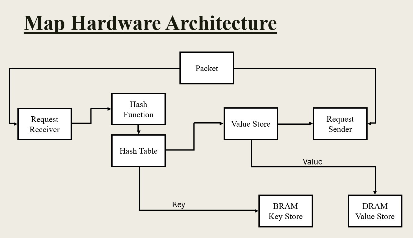
developed for various industry level projects. Database accelerators using FPGA is the
active and growing with digital team in CVEST.
Datacenter workloads demand high computational capabilities, flexibility, power efficiency, and low cost. It is challenging to improve all of these factors simultaneously. To advance data center capabilities beyond what commodity server designs can provide, we are working on designing and building a composable, reconfigurable system to accelerate portions of large-scale database services.

The research work is on the efficient VLSI implementation of the Fast Fourier Transform algorithms. Tangent FFT algorithms have very low arithmetic complexities and that can be used for efficient VLSI implementations of FFT cores. Even though the Tangent FFT algorithms have very low arithmetic complexities their implementations are very less explored. Choosing an appropriate hardware is important to get the advantage of the low arithmetic complexities of Tangent FFT's during implementation.
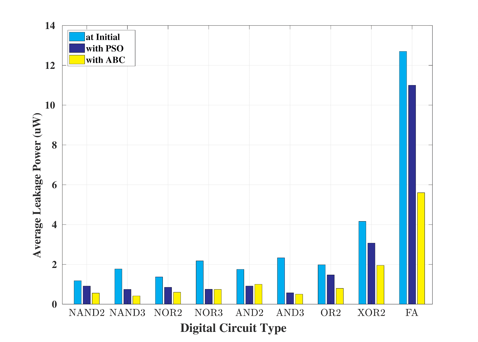
Optimal Transistor Sizing to Reduce Leakage & Delay for Digital Circuits: As per ITRS for the trend of power dissipation with respect to technology progress, static power dissipation in CMOS is expected to exceed dynamic power dissipation.
Generally any circuit will have some
static leakages when the circuit is not switching states. The approach is to reduce
these static leakages and switching delays using Machine Learning Algorithms by changing
the dimensions of the individual devices (W/L) of the corresponding circuits.
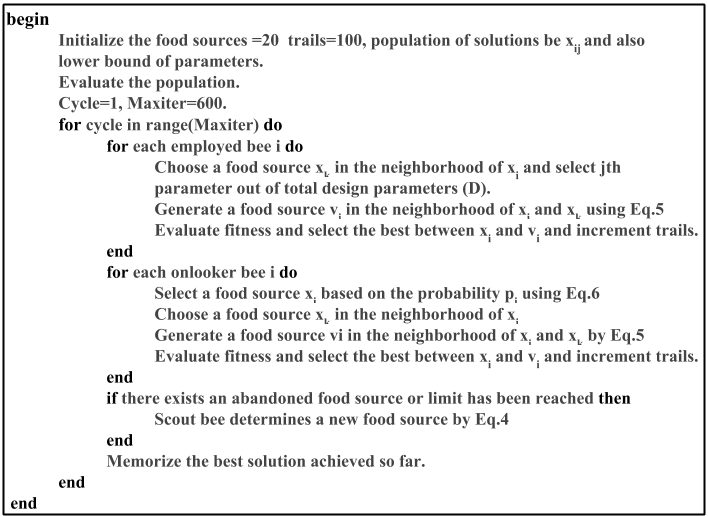
Thus here in CVEST, we implement
different algorithms such as Genetic algorithm, Particle Swarm Optimization,
Artificial Bee Colony, Simulated Annealing etc to find the PVT variations aware robust
transistor sizing of the
circuits for minimum leakage power dissipation, propagation delay and area. The yield
calculation is then done
with the Monte Carlo analysis.

Digital circuits are made up of smaller sub-circuits like gates (AND,NOT, NOR, XOR,
NAND, AND, MUX) , Adders( Full Adder, Half Adder , Ripple Carry Adder ) , Multipliers
etc. There are multiple devices in each of these circuits. Generally any circuit will
have some static leakages when the circuit is not switching states.
The approach is to reduce these static
leakages and switching delays using Machine Learning Algorithms by changing the
dimensions of the individual devices (W/L) of the corresponding circuits. Evolutionary
Multi-objective Algorithms like Memetic Algorithm , Genetic Algorithm, Strength Pareto
Evolutionary Algorithm , Simulated Annealing as well as Swarm Based Algorithms like
Particle swarm optimization, Artificial bee colony algorithm , Ant colony optimization
algorithms have successfully been implemented in solving these multi-objective
optimization problems. Apart from working under normal conditions , the algorithms also
takes into account the variation in several process parameters ( Threshold Voltage ,
Mobility, Width and Length Offset and man more) to ensure optimized performance even in
case of non-uniformity in the fabrication of deep sub-micron digital circuits.
Also external working conditions such as
operating temperature(-55oC to 125oC) , Supply Voltage variations (0.9V – 1.1V) are also
considered so that the performance is not much affected in case of such external
environmental variations. Techniques have been applied in 45nm , 32nm and 22nm
technology circuits achieving remarkable
results. The bigger objective is building a framework of effective algorithms that would
provide optimum results within a very short span of time as compared to manual
optimization. To minimize the time taken further, effective model development for
devices are being done. The main motivation behind model development is to do skip
calling SPICE tools for simulations but still get extremely accurate results after
proper initial training of the model. The main advantage is the time required to get the
results is negligible as compared to SPICE simulations .